|
J-Testr Customized RF Solutions
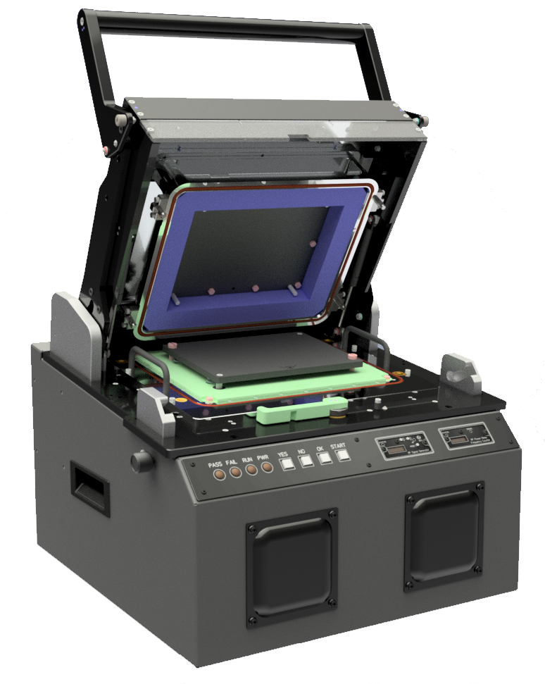
Customized RF solutions allow the testing of the latest integrated RF devices for the Internet of Things (Bluetooth, LORA, WIFI, etc.) and other RF applications (e.g. ISM 433MHz). These test solutions provide a small footprint, cost effective pricing, advanced features and flexibility that enable large and small companies to effectively test their RF devices with confidence and dramatically improve the quality of testing at the printed circuit board assembly (PCBA) stage.
All the equipment fits neatly inside our Midi or Max fixture base box and requires no external test equipment. The only support equipment that is required is a PC. |
|
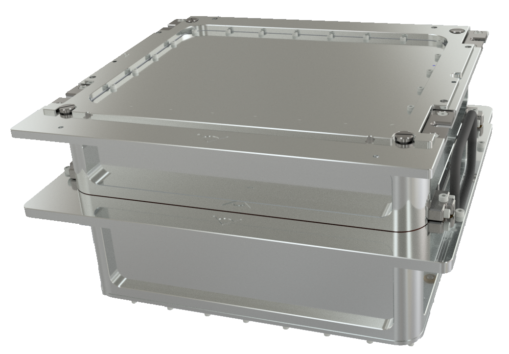
Customized RF solutions incorporates a full fixture Exchangeable Unit and bed of nails capability within a high isolation RF chamber, which shields the RF device, and its measurements, eliminating the need for special ‘low RF noise’ rooms within a production environment and providing high quality and repeatable measurements. The Exchangeable Unit has been designed for ease of integration with open access to the RF chamber and can be expanded to increase the RF test environment. ‘All-round’ absorbing material can be fitted to enable measurement of RF transmitting devices while reducing reflected signals.
|
|
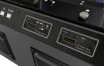
Depending on the RF application we are able to integrated RF instruments that are accessible via the front user panel which allows control both manually and/or automatically with test sequencer software. This allows quick testing or debugging of a RF devices with little or even no test software support. The RF instruments include comprehensive digital displays allowing RF signal measurements/outputs to be monitored in real-time, for example, during an automated test.
|
Testing
Our customized RF solutions allow standard functional testing, of the UUT, as well as fully testing and characterization of the RF signal path and RF oscillator circuits. This means that the solution can detect:
If the receiver part of the circuit is required to be tested, then this can be done with a simple ‘signal repeater’ circuit inside the RF chamber or with a integrated RF generator if better characterization is required.. Please see article ‘Testing of SOC based RF Devices’ for more details.
- RF path impedance mismatches (caused by solder joint or PCB antenna issues)
- Incorrectly fitted tuned components (like RF filters, balun, etc)
- Frequency generation inaccuracies (badly soldered, damaged or incorrectly fitted crystal)
If the receiver part of the circuit is required to be tested, then this can be done with a simple ‘signal repeater’ circuit inside the RF chamber or with a integrated RF generator if better characterization is required.. Please see article ‘Testing of SOC based RF Devices’ for more details.
Cabling
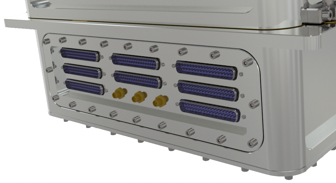
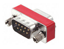
Power, stimulation and RF connections are easily connected through to the UUT inside the RF chamber via a cable entry bulkhead, at the rear of the lower RF chamber, using D-Sub connectors similar to that shown below:
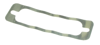
D-Sub connectors are perfect to cross the RF connection bulkhead as they are metal, have RF gaskets available and, if needed, have RF signal filters available either inside the connector or as an adaptor to make excellent RF barrier to the outside of the RF chamber.

