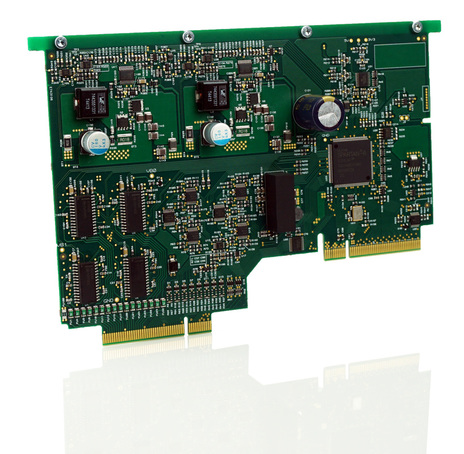
HV IO Peripheral Card
Features• 32 High-voltage outputs (2 banks of 16)
• High-side, low-side & push-pull drive capable • Fully adjustable voltage supply per bank (5V to 30V) • 350mA source current per output (3A total per bank) • Accurate measurement of bank PSU voltage/current • Overload protection • 32 High-voltage inputs (2 banks of 16) • Programmable threshold of 0.1V to 28V per bank • High impedance inputs (no R divider) with hysteresis • Input over-load protection • JTAG or Ethernet controlled • 8 User I/Os with UART, SPI, I2C, PWM, GoJ-Safe & GPSM features |
| ||
About
The HV IO peripheral card gives the user 32 high-voltage & high-current outputs that are High-Side, Low-Side & Push-Pull drive capable. Also there are 32 High Voltage inputs with adjustable thresholds and with hysteresis. These can be controlled from either the Ethernet communications or from a boundary scan bus/chain. This allows the user ultimate flexibility to use the card within an Ethernet controlled system, or to make full utilization of the powerful IO testing features provided by some JTAG testing tools.
The outputs are arranged in two banks of 16, each bank having independently programmable supply voltages, from 5V to 30V, and each bank having high current capability up to 350mA per IO (maximum 3A total per bank). The high current capability allows direct driving of relays & solenoids, or could even be used to power multiple small circuits.
Protected adjustable power supplies, per bank, are integrated on the card to save the user from providing the output voltages externally. These supplies enable the user to dynamically control the output voltages, allowing testing at different voltage levels, hence achieving better test coverage. An accurate high resolution 16 bit measurement system is also included to enable verification (self-test) of the output voltages, and also, the output current delivered to the UUT circuitry from the outputs.
The inputs can tolerate voltages from 0V to 30V with a programmable accurate threshold voltage from 0.1V to 28V per bank. This allows the user to select the voltage level for sensing a logic '0' and a logic '1'. The adjustable threshold allows the user to test the UUT voltage driver meets the required output specification without the use of a separate measurement.
All inputs incorporate hysteresis, for a clean logic transition.
All inputs also have true high input impedance (i.e. do NOT have resistive dividers like some designs). This allows the user to fit external resistor dividers, if required, to achieve a much higher input voltage range.
With 'test in mind' all input and output lines are protected against over-voltage and over-current as it is never known what voltages or currents untested UUTs could present to these lines. A global IO enable line allows the user to 'float' the IO lines until the UUT is fully powered.
Finally, as with all bus connected peripherals, the ADC/DAC peripheral provides 8 general purpose User IOs which can be used to control and/or read custom circuitry on the interposer. The IOs can provide special hardware functions such as 16-bit PWM, UART, SPI, I2C and GPSM (General Purpose Signal Monitor for measuring freq/duty/pulse-width etc.) that can be multiplexed to any of the IO pins.


